半导体制造中的ID读取与可追溯性
突破低对比度与表面变化限制,实现ID读取精度最大化
可追溯性是半导体制造的核心要素。Basler视觉方案可实现从晶圆边缘OCR、FOUP条码、掩膜版ID、基板编码到载具环标记的全流程精准标识读取,确保各生产环节的可靠追踪。
实现从晶圆到最终封装的全流程可靠标识读取
在半导体制造全流程中,需稳定读取各类标识码以维持完整可追溯性。这些标识包括激光蚀刻、点刻或印刷于不同光学特性表面的条形码、OCR字符、DataMatrix码及二维码。

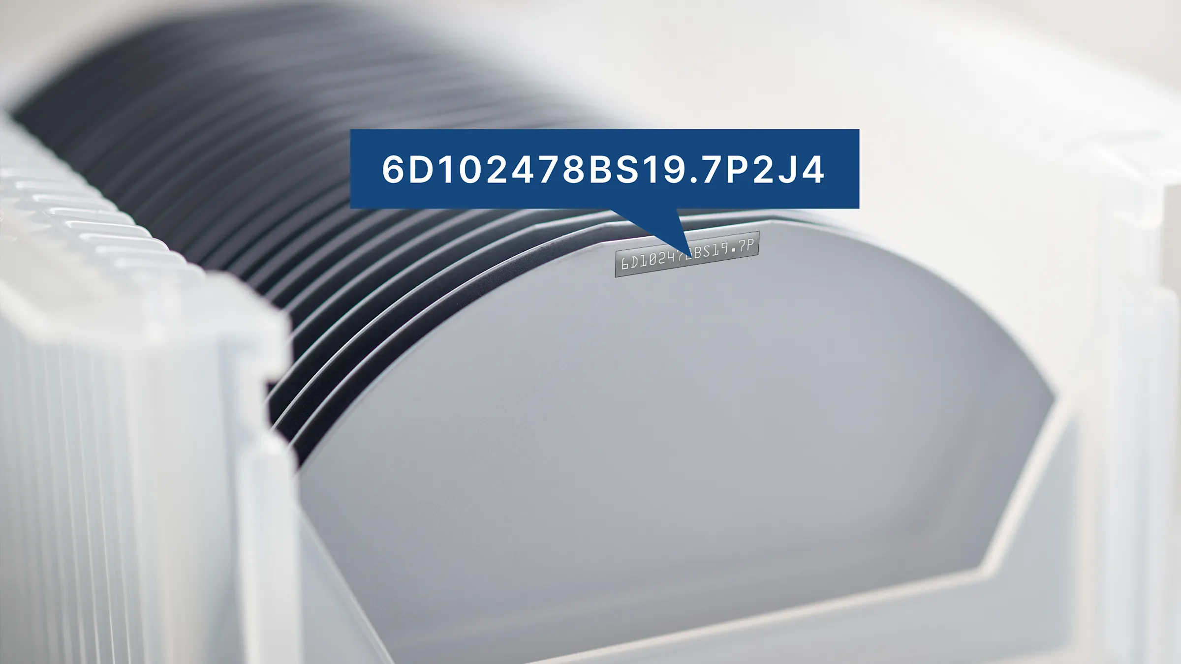
Wafer and reticle ID reading
Wafer edge OCR involves reading small alphanumeric characters laser-marked on the outer edge of a silicon wafer. These unique IDs typically follow industry standards such as SEMI M12 or T7 and are essential for traceability throughout the manufacturing process.
Reticles, or photomasks, contain the circuit pattern for each chip layer. A laser-etched ID on the glass or chrome border ensures proper usage and traceability during lithography.

Carrier ring and chip tray reading
Post-dicing, wafers are transferred to carrier rings or substrates for downstream processes such as die attach, wire bonding, and packaging. These components are marked with process-specific IDs that enable traceability of individual dies or batches during handling and assembly. However, reading these IDs reliably poses unique vision challenges due to material properties, surface wear, and environmental variability common in back-end environments.
Basler半导体ID读取集成化视觉方案
Basler推出可配置的视觉方案,专为半导体ID读取设计,可无缝集成至检测、切割及搬运系统中。该方案整合四大核心组件:高性能相机、优化光学系统、自适应光源及智能软件工具,协同实现晶圆边缘OCR、载具环编码及基板ID的灵活可靠读取。此集成架构确保在多样材料、光照条件及工艺环境中均能输出稳定结果,全面满足先进封装领域对追溯系统的严苛要求。
近期,越来越多客户采用受光度技术启发的高级多角度成像策略,但系统设计、软件集成及实施方法的差异仍持续带来技术挑战。

继续阅读用例
填写表单以阅读完整用例。内容将在提交表单后立即提供。