线阵相机中的TDI:选择模拟技术还是数字技术?
检测快速移动表面上的微小缺陷,需要在不降低生产速度的前提下实现高灵敏度。时间延迟积分(TDI)技术可在保持吞吐量的同时,增强来自移动物体的信号。本指南介绍了两种主要的TDI技术方案,以及如何为半导体、显示器、印刷电路板(PCB)和卷材检测选择合适的方法。
最后更新: 2026/03/25
阅读时间:约 21 分钟
导言与概述
线阵相机每次仅采集一条窄线,用于拍摄快速移动的物体,因此非常适合晶圆、玻璃面板、印刷电路板以及卷装材料的检测。与面阵相机不同,线阵相机能够生成无失真、长度无限的图像。在高速运行时,由于每行的曝光时间缩短至微秒级,导致在低反射率表面(例如仅反射约4%光线的裸硅)上获得噪声较大的图像。
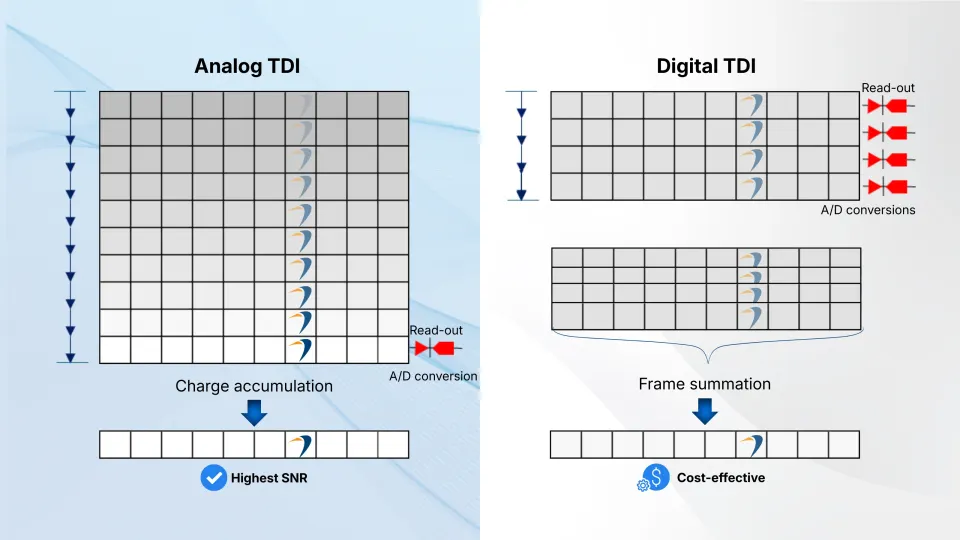
在物体上的每个点经过芯片时,时间延迟积分(TDI)技术通过对其进行多次曝光,并将这些曝光累加起来,从而解决上述问题。市面上主要有两种TDI技术路线:
模拟式TDI芯片:采用CCD或混合CMOS技术,在32级至200多级之间进行模拟信号累加。
数字式TDI芯片(多线CMOS + FPGA):使用带有四行像素的CMOS芯片,并在相机的FPGA中进行数字累加。
这两种方法均旨在提高高速线阵成像中的光线灵敏度与图像亮度,但它们在架构、可实现的灵敏度以及系统成本方面存在显著差异。理解这些差异有助于工程师确定哪种TDI方案最符合其检测需求。
TDI基本原理:实现灵敏度的两种途径
模拟式TDI芯片
模拟式TDI芯片在芯片的电荷域中直接累加信号。芯片由一条分为多级(通常为32至256级)的像素列构成。当物体移动时,光生电荷与运动同步逐级转移,并在模数转换前完成累加。
由于信号积分在模拟域进行,读出噪声仅在最终模数转换时引入一次。这使得灵敏度得到显著提升,并获得了极高的信噪比性能,从而在极低照度(通常 ≤ 0.1勒克斯)条件下仍能可靠成像,同时保持较低的功耗(通常为2-4瓦)。
随着级数增加,物体移动与电荷转移之间的同步要求也愈发严格。因此,高阶TDI芯片需要极其精确的运动控制与编码器反馈。如果物体速度与行频之间出现任何不匹配,都会导致图像模糊。
Digital TDI
Digital TDI uses a CMOS sensor with four parallel rows. As the object moves past the sensor, each row captures the same scene at slightly different moments. The camera’s FPGA aligns the rows through spatial correction and digitally combines the pixel data.
By accumulating multiple exposures of the same moving object, digital TDI improves light sensitivity and image brightness in high-speed line-scan imaging. Because each row is digitized before summation, read noise is introduced at every stage, limiting the achievable sensitivity gain when compared with analog TDI.
Each row undergoes independent A/D conversion prior to accumulation. High-quality A/D conversion and digital signal processing help minimize signal loss and preserve image quality during digital summation.
Like analog TDI, digital TDI requires accurate matching between object speed and line rate. Small speed variations (approximately ±5–10%) can be tolerated through FPGA-based spatial correction, but larger mismatches will still cause image blur.
技术比较与关键性能驱动因素
如上一节所述,模拟式与数字式TDI的主要区别在于信号累加发生的位置。下表通过对性能相关参数的深入比较,进一步阐述这些差异。
参数 | 数字式TDI (模数转换后) | 模拟式TDI (电荷域) | 对工程师的意义 |
积分域 | 数字域(FPGA求和/模数转换后) | 模拟域(电荷转移/模数转换前) | 决定了基础噪声本底与增益机制。 |
|---|---|---|---|
典型级数/行数(N) | 低(通常为4行) | 高(32-256级) | 决定了可实现的最大光线灵敏度。 |
读出噪声累加 | 引入N次(在每行读出时) | 仅在最终输出端引入一次 | 实现最大化的灵敏度: 在弱光条件下,模拟式TDI可获得的信噪比增益 ≈ √N。 |
可用照度范围 | 中等弱光(≥ 0.5勒克斯) | 极弱光(≤ 0.1勒克斯) | 对暗场/电致发光应用至关重要。 |
运动容差 | 对小幅速度波动容忍度较高 | 需严格同步 | 影响机械集成与编码器要求的复杂度与成本。 |
光谱能力 | 内置色彩/多光谱支持 | 通常为黑白,以获得最大信噪比(SNR)。 | 对PCB检测等需要彩色信息的应用是一大优势。 |
相对系统成本 | 较低(标准CMOS芯片、机械要求宽松) | 较高(专用混合芯片、高精度机械装置) | 预算限制往往是第一项筛选条件。 |
脚注:
在TDI成像中,理想情况下信号的增加与级数(N)成正比。
对于TDI芯片,由于读出噪声是仅在最终输出端引入一次,因此噪声增加较慢(仅增加√N)。
对于数字式TDI,每行读出时均引入读出噪声,因此总噪声增长更快,从而限制了在弱光条件下的有效信噪比增益
需要协助您选择合适的TDI架构吗?
即刻与Basler视觉专家讨论您的检测要求,针对您的光源、应用速度和灵敏度限制找到出色视觉方案。
与视觉专家对话无论采用何种实现方式,TDI的根本目的都是在高速线阵成像中提高光线灵敏度与图像亮度。数字式TDI为那些仅需较少级数(例如四行)即可满足要求的应用提供了额外的选择。在这些情况下,与专用的TDI芯片相比,客户能够以更具成本效益的方案获得显著的亮度与灵敏度提升。

应用实例


战略决策矩阵与检查清单
选择出色的TDI架构,无论是具备数字式TDI功能的灵活多线CMOS,还是高灵敏度的TDI芯片,都要求工程师妥善综合考虑相机性能与应用的局限性。这一决策通常由三个主要因素决定:可用的光设备预算、系统对机械同步稳定性的容忍度、以及总体成本上限。下表列出了一个实用核对清单,助您将核心应用需求映射到合适的TDI技术。
要求 | 数字式TDI | 模拟式TDI |
预算有限,对成本极敏感 | 首选 | 受限 |
|---|---|---|
光照强度 ≥ 0.5勒克斯 | 首选 | 可接受 |
传送速度有一定波动(例如 ±5%) | 首选 | 受限 |
光照强度 ≤ 0.5 勒克斯(通常 ≤ 0.1) | 受限 | 首选 |
检测亚微米裂纹、微弱残留或电致发光 | 受限 | 首选 |
裸硅暗场检测 | 受限 | 首选 |
将洁净室的发热量降至最低 | 可接受 | 首选 |
可接受黑白成像 | 可接受 | 首选 |
总结
For applications that do not require the extreme sensitivity of a dedicated TDI sensor, digital TDI provides a practical way to improve light sensitivity and image brightness in high-speed line-scan imaging.
Analog TDI sensors (especially the new back-illuminated hybrid CMOS generation) remain the only choice when ultimate sensitivity under minimal illumination is required, such as front-end wafer inspection or sub-100 nm defect detection.
Key takeaways for system engineers:
Digital TDI is often a practical starting point when moderate sensitivity improvement is sufficient and system cost must remain controlled.
Move to analog TDI when the system becomes truly light-limited: Transition only if proof-of-concept testing shows you are genuinely light-limited below ~0.3 lux.
Future-proofing: The newest hybrid TDI cameras are rapidly closing the speed gap and deserve consideration for future-proof designs requiring maximum sensitivity.
Validation is key: Choose based on your actual light budget, spectral needs, and motion stability, then validate with a short on-line trial. The right TDI technology will dramatically improve yield and throughput.
不确定哪种TDI方法适合您的系统?
Send us your inspection requirements and we can help evaluate the optimal imaging architecture.
TDI技术常见问题
不会。TDI并不提高相机的行频,而是在维持高检测速度的前提下,提升光线灵敏度与图像亮度。
TDI依赖于物体运动与芯片电荷转移(或曝光时序)之间的精确同步。如果物体速度与行频不匹配,累加的信号将发生错位,导致图像模糊。
即使是数字式TDI,物体速度也必须与相机的行频紧密匹配。由于需要合并多次曝光,每一行都必须在正确的时间采集到运动物体上的同一点。如果速度不匹配,累加的信号将发生错位,图像便会模糊。
要点:
数字式TDI ≠ 普通线阵技术
同步要求与TDI类似
区别在于积分发生的位置,而不是运动要求
微小的速度变化有时可以通过基于FPGA的空间校正进行补偿,但较大的偏差仍会导致图像模糊。
当检测受到可用光线严重限制,或必须检测极微弱缺陷时,通常优先选用专用的TDI芯片,例如:
暗场晶圆检测
电致发光检测
检测对比度极低或亚微米级缺陷
在这些情况下,模拟式TDI能够提供最高的信噪比性能。
然而,最佳选择往往取决于整个成像系统,包括:
可用光源
光学与放大倍数
运动稳定性
缺陷对比度
这些因素都可能影响数字式TDI是否足以满足需求,或者是否需要TDI芯片。在实践中,通常建议进行评估与测试。